ÎÅäÏûÑÏóÜÏù¥ ÏßÑÌôîÌïòÎäî Î∞òÎèÑÏ≤¥ ÏÇ∞ÏóÖ ÌôòÍ≤ΩÏóêÏÑú Ïû¨Î£å Í≥ºÌïôÏùò Î∞úÏÝÑÏùÄ ÏѱÎä•, Îǥ͵¨Ïѱ Î∞è ÏÝïÎ∞ÄÎèÑÏùò ÏÉàΰúÏö¥ ÏßÄÌèâÏùÑ Ïó¨Îäî Îç∞ ϧëÏ∂îÏÝÅÏù∏ Ïó≠ÌïÝÏùÑ Ìï©ÎãàÎã§. Ïù¥Îü¨Ìïú ÌöçÍ∏∞ÏÝÅÏù∏ Í∞úÎ∞ú ϧëÏóêÏÑú Í¥ëÌïô Îì±Í∏â ÏÑùÏòÅ ÌäúÎ∏åÎäî ϵúÏ≤®Îã® Í∏∞ÏàÝÍ≥º Ïû¨Î£å ÏàúÎèÑÏùò ÏúµÌï©ÏùÑ Î≥¥Ïó¨Ï£ºÎäî ϶ùͱ∞ÏûÖÎãàÎã§. Ïù¥ Í∏∞ÏǨÏóêÏÑúÎäî Í¥ëÌïô Îì±Í∏â ÏÑùÏòÅ ÌäúÎ∏åÏùò ÏàòÎßéÏùÄ Ïû•ÏÝê, ÏùëÏö© Î∂ÑÏïº, Í≥ºÏÝú, ÌòÅÏãÝ Î∞è ÎØ∏Îûò ÏÝÑÎßùÏùÑ ÏûêÏÑ∏Ìûà ÏÇ¥Ìé¥Î≥¥Í≥Ý Í≥ÝÍ∏â Î∞òÎèÑÏ≤¥ Î∂ÄΨ∏ÏùÑ ÌòÅÏãÝÌïòÎäî Îç∞ ÏûàÏñ¥ ϧëÏ∂îÏÝÅÏù∏ Ïó≠ÌïÝÏùÑ Í∞ïÏ°∞Ìï©ÎãàÎã§.
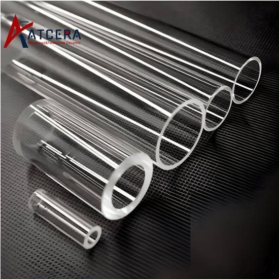
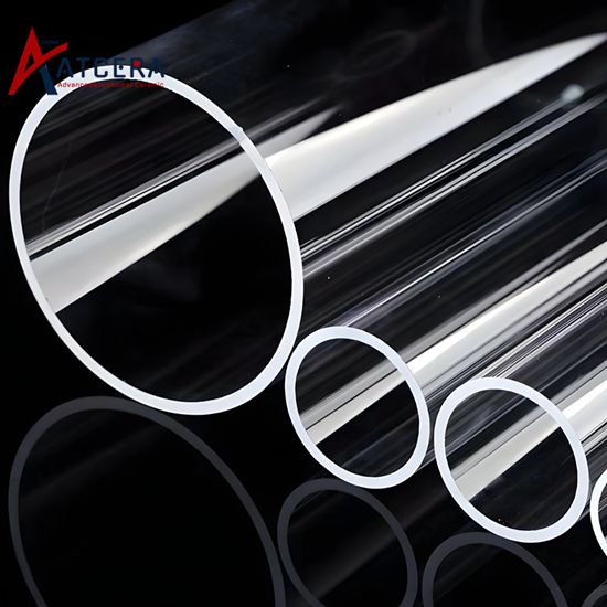
Í¥ëÌïô Îì±Í∏â ÏÑùÏòÅ ÌäúÎ∏åÏùò Ïû•ÏÝê
Ï¥àÏàúÏàòÌïòÍ≥Ý ÏÑ∏Ïã¨ÌïòÍ≤å Í∞ÄÍ≥µÎêú ÏÑùÏòÅÏúºÎ°ú ÏÝúÏûëÎêú Í¥ëÌïô Îì±Í∏â ÏÑùÏòÅ ÌäúÎ∏åÎäî ÌïòÏù¥ÌÖåÌŨ ÏùëÏö© Î∂ÑÏïºÏóê ÏóÜÏñ¥ÏÑúÎäî ÏïàÎêÝ ÌäπÏѱÏùò ÎπÑ͵êÌïÝ Ïàò ÏóÜÎäî Ï°∞Ìï©ÏùÑ ÏûêÎûëÌï©ÎãàÎã§. Îõ∞Ïñ¥ÎÇú Í¥ëÌïô ÏÑÝΙÖÎèÑ, ÎÜíÏùÄ Ïó¥ ÏïàÏÝïÏѱ Î∞è ÎÇÆÏùÄ Ïó¥ÌåΩÏ∞Ω Í≥ÑÏàòÎäî Ïò®ÎèÑ Î≥ÄÎèôÏóê ÎåÄÌïú ÏÝïÎ∞ÄÌïú ÏÝúÏñ¥Î•º Î≥¥Ïû•ÌïòÍ≥Ý ÏôúÍ≥°ÏùÑ ÏµúÏÜåÌôîÌïòΩ∞ Í≥µÏÝï ÏÝïÌôïÎèÑΕº Ìñ•ÏÉÅÏãúÌǵÎãàÎã§. ÎòêÌïú ÌôîÌïôÏÝÅ Î∂ÄÏãù Î∞è Î∞©ÏǨÏÑÝ ÏÜêÏÉÅÏóê ÎåÄÌïú ÏÝÄÌï≠ÏѱÏùÄ Ïó¥ÏïÖÌïú ÌôòÍ≤ΩÏóêÏÑúÏùò Îǥ͵¨ÏѱÏùÑ Í∞ïÏ°∞ÌïòÏó¨ ÍπåÎã§Î°úÏö¥ Î∞òÎèÑÏ≤¥ ÏÝúÏ°∞ Í≥µÏÝïÏóê Ïù¥ÏÉÅÏÝÅÏûÖÎãàÎã§.
광학 등급 석영 튜브의 응용
Í¥ëÌïô Îì±Í∏â ÏÑùÏòÅ ÌäúÎ∏åÏùò Îã§ÏñëÏѱÏùÄ Î∞òÎèÑÏ≤¥ ÏÇ∞ÏóÖ Ïùò Ïó¨Îü¨ Ï∏°Î©¥Ïóê ͱ∏Ï≥ê ÏûàÏäµÎãàÎ㧠. Ïù¥Îäî ϧëÏöîÌïú ÏÝúÏ°∞ Îã®Í≥ÑÏóêÏÑú ÏàúÎèÑÍ∞Ä ÏµúÏÜåÌïúÏùò Ïò§ÏóºÏùÑ Î≥¥Ïû•ÌïòÎäî Ïõ®Ïù¥Ìçº ÏóêÏπ≠ Î∞è ϶ùÏ∞© ϱîÎ≤ÑÏóêÏÑú ϧëÏöîÌïú Ïó≠ÌïÝÏùÑ Ìï©ÎãàÎã§. ÎòêÌïú Ï∞Ω, ÎÝå϶à Îì±Ïùò Í¥ëÌïô Î∂ÄÌíàÏóê ÏǨÏö©ÌïòΩ¥ ÏÝïÎ∞ÄÌïú Îπõ ÏÝÑÏÜ°ÏùÑ Í∞ÄÎä•ÌïòÍ≤å ÌïòÏó¨ Ìè¨ÌÜÝζ¨ÏÜåÍ∑∏ÎûòÌîº Í≥µÏÝïÏùò Ìö®Ïú®ÏѱÏùÑ Ìñ•ÏÉÅÏãúÌǵÎãàÎã§. Ïö©Í¥ëΰú Î∞è Î∞òÏùëÍ∏∞Ïóê ÌܵÌï©ÌïòΩ¥ Ïò®ÎèÑÏóê ÎغÍ∞êÌïú Ìï©Ïѱ Î∞òÏùëÏù¥ Ï¥âÏßÑÎêòÏñ¥ Î∞òÎèÑÏ≤¥ Ïû•ÏπòÏö© Ï≤®Îã® ÏÜåÏû¨ ÏÉùÏÇ∞ÏùÑ Îí∑Î∞õÏπ®Ìï©ÎãàÎã§.
Ï≤®Îã® Î∞òÎèÑÏ≤¥ÏóêÏÑú Í¥ëÌïô Îì±Í∏â ÏÑùÏòÅ ÌäúÎ∏åÏùò Ïó≠ÌïÝ
Í≥ÝÍ∏â Î∞òÎèÑÏ≤¥ ÏòÅÏó≠ÏóêÏÑú Í¥ëÌïô Îì±Í∏â ÏÑùÏòÅ ÌäúÎ∏åÎäî ÏÜåÌòïÌôî Î∞è ÏѱÎä•Ïùò Í≤ΩÍ≥ÑΕº ÎÑìÌûàÎäî Îç∞ ϧëÏöîÌïú Ïó≠ÌïÝÏùÑ Ìï©ÎãàÎã§. ͵¨Ï°∞ÏÝŠΨ¥Í≤∞ÏѱÏùÑ ÏúÝÏßÄÌïòΩ¥ÏÑú Í∑πÌïúÏùò Ïò®ÎèÑΕº Í≤¨Îîú Ïàò ÏûàÎäî Îä•ÎÝ•ÏùÄ ÏïÑÏ£º ÏûëÏùÄ Ìé∏Ï∞®ÎùºÎèÑ Í∏∞Îä•ÏùÑ ÏÝÄÌïòÏãúÌǨ Ïàò ÏûàÎäî Ï∞®ÏÑ∏ÎåÄ ÎßàÏù¥ÌŨΰúÏπ© Í∞úÎ∞úÏóê ÎߧÏö∞ ‚Äã‚ÄãϧëÏöîÌï©ÎãàÎã§. Î∞òÎèÑÏ≤¥ ÌòïÏÉÅÏù¥ Ï∂ïÏÜåÎêòÍ≥Ý Ï≤òζ¨ Î≥µÏû°ÏѱÏù¥ ϶ùÍ∞ÄÌï®Ïóê Îî∞Îùº Í¥ëÌïô Îì±Í∏â ÏÑùÏòÅ ÌäúÎ∏åÏóê ÎåÄÌïú ÏùòÏ°¥ÎèÑÍ∞Ä ÎÜíÏïÑÏÝ∏ ϵúÏ≤®Îã® Í∏∞ÏàÝÏóê ÌïÑÏöîÌïú ÏÝïÎ∞ÄÎèÑÏôÄ ÏãÝ΢∞ÏѱÏù¥ Î≥¥Ïû•Îê©ÎãàÎã§.
Í¥ëÌïô Îì±Í∏â ÏÑùÏòÅ ÌäúÎ∏å ÌôúÏö©Ïùò Í≥ºÏÝú
Despite their numerous advantages, the utilization of High-Purity Optical Quartz Tubing presents challenges, notably in terms of cost and availability. The stringent requirements for purity and precision drive up production costs, while maintaining a consistent supply chain can be daunting due to the rarity and complexity of raw materials. Additionally, integrating these tubes into advanced manufacturing processes often necessitates specialized equipment and expertise, posing barriers to entry for some manufacturers.
Innovations and Research in Optical Grade Quartz Tubes
Ongoing research and development efforts focus on enhancing the properties of Precision Grade Optical Quartz Tubes further, aiming to reduce costs, improve production efficiency, and expand their applicability. Advances in nanotechnology and precision engineering are enabling the creation of thinner, stronger, and more optically transparent tubes. Moreover, the exploration of alternative quartz sources and recycling strategies aims to mitigate supply chain constraints and environmental impacts.
Manufacturing and Production of Optical Grade Quartz Tubes
The manufacturing process of Optical Grade Quartz Tubes is meticulous, involving the purification of raw quartz to ultra-high purity levels, by precise shaping and polishing. Advanced manufacturing techniques, such as chemical vapor deposition and plasma-assisted processes, enable the creation of complex structures with unparalleled surface quality. Stringent quality control measures ensure that every tube meets the rigorous standards demanded by the semiconductor industry.
Future Prospects of Optical Grade Quartz Tubes in Advanced Semiconductor
Looking ahead, Optical Grade Quartz Tubes hold immense promise for advancing the semiconductor industry. As Moore's Law approaches its physical limits, the need for innovative materials and processes intensifies. Optical Grade Quartz Tubes, with their unique combination of properties, are poised to play a pivotal role in enabling the development of smaller, faster, and more energy-efficient semiconductor devices. Their integration into emerging technologies, such as 3D printing for semiconductor manufacturing, will further accelerate this progression.
Comparison with Other Semiconductor Materials
While other materials, such as silicon carbide and alumina, offer their own sets of advantages in semiconductor applications, Optical Grade Quartz Tubes stand out for their unparalleled optical clarity, thermal stability, and chemical resistance. These properties, coupled with their ability to withstand extreme processing conditions, make them invaluable for tasks that require a higher degree of precision and control.
Conclusion: The Potential of Optical Grade Quartz Tubes in Revolutionizing the Semiconductor Industry
Í≤∞ΰÝÏÝÅÏúºÎ°ú, Í¥ëÌïô Îì±Í∏â ÏÑùÏòÅ ÌäúÎ∏åÎäî Í∏∞ÏàÝ Î∞úÏÝÑÏùÑ Ï¥âÏßÑÌïòÎäî ÌûòÏùÑ ÏßÄÎãå Î∞òÎèÑÏ≤¥ ÏÇ∞ÏóÖÏùò ϧëÏ∂îÏÝÅ ÌòÅÏãÝÏùÑ ÎÇòÌÉÄÎÉÖÎãàÎã§. ÏßÄÏÜçÏÝÅÏù∏ Ïó∞͵¨ Î∞è Í∞úÎ∞úÍ≥º Í≤∞Ìï©Îêú Í≥ÝÏúÝÌïú ÌäπÏѱÏùò Ï°∞Ìï©ÏùÄ Ï∞®ÏÑ∏ÎåÄ ÎßàÏù¥ÌŨΰúÏπ© Î∞è Ïû•ÏπòΕº Ï∂î͵¨ÌïòÎäî Îç∞ ÌïÑÏàòÏÝÅÏù∏ ͵¨Ïѱ ÏöîÏÜåΰú Ïûêζ¨ÎߧÍπÄÌï©ÎãàÎã§.